3 Cost-Efficiency Strategies in Semiconductor Construction: Balancing Innovation and Quality
The semiconductor manufacturing industry faces significant challenges in controlling costs as material prices rise significantly. The manufacturing process grows increasingly complex, leaving little room for error.
- Constructing semiconductor fabrication facilities (fabs) typically costs between $1-20 billion per facility.
- Due to these substantial expenses, projects can easily fall into overspending.
These facilities require advanced construction techniques to meet the industry’s ever-growing demands for innovation, precision, and quality. Each fab is equipped with thousands of multimillion-dollar tools essential for chip manufacturing. To keep up with the high demand for semiconductors, companies must adopt creative and effective cost-saving measures.
In this article, we explore three strategies that companies are implementing to construct these factories more efficiently while still maintaining production quotas and quality standards.
Strategy 1: Modular Construction and Prefabrication – Intel’s Fab 42 in Arizona

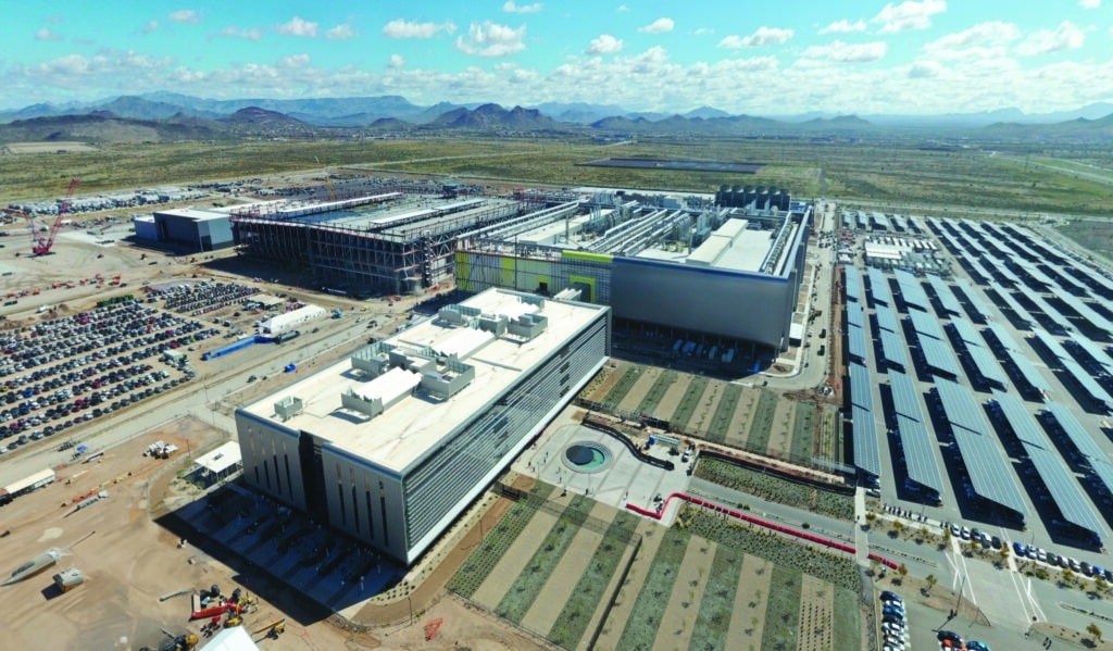
Intel’s use of modular construction at its Arizona Fab 42 facility highlights how prefabrication can significantly reduce construction costs without compromising quality. Modular construction involves building large components off-site and then transporting them to the fab for installation. By prefabricating utility racks and assemblies off-site, Intel reduced on-site congestion, a common issue when multiple teams and contractors work simultaneously. This approach not only accelerated the construction timeline by 60% but also saved $25 million.
Prefabrication and modular assembly minimize unnecessary labor hours on-site, allowing construction teams to focus on higher-priority tasks and critical elements of the build. The long-term effects extend beyond initial savings, as increased efficiency frees up resources for other investments in innovation and quality control.
Intel’s example demonstrates how modular construction can cut costs and streamline processes while maintaining the high standards required for semiconductor manufacturing.
Strategy 2: Automation-Driven Efficiency – Samsung’s Pyeongtaek Campus, South Korea
_Samsung_Pyeongtaek_Line_2%2520(1).jpeg)
Samsung's massive Pyeongtaek campus in South Korea is one of the largest semiconductor manufacturing facilities globally. It serves as a example of effectively leveraging automation to achieve optimal cost efficiency in fab construction.
Integrated Supply Chain Management
Seamless delivery of materials is critical in the fab construction process. Samsung implemented an advanced supply management system that not only ensures efficient resource allocation but also reduces delays and over-scoping.
Reduction in over scoping: While over scoping ensures that all the materials are available at the right time for a project, the costs can build up. A project can end up buying hundreds more electrical panels which are only loaded to 10% of capacity - resulting in millions of dollars of overspending. Samsung's approach mitigated such overspending by tailoring material procurement to precise project requirements.
Efficient Coordination: By integrating suppliers directly into their advanced planning system, Samsung streamlined procurement processes. This ensured that construction resources were available precisely when needed, minimizing storage costs and avoiding delays.
Energy-Efficient Design and Construction
In addition to Automation Samsung also had energy efficiency in mind when whet built their fab this approach not only promoted efficient use of tooling and materials during construction but would also prepared the fab for sustainable, long-term operations.
Heat Recovery Ventilation (HRV) Systems: Installed across all areas of the facility, the HRV system utilizes artificial intelligence to capture and recycle waste heat from the exhaust systems. This heat is then reuses to preheat incoming air. The system intelligently detects where heat is needed and diverts it accordingly, reducing heating energy demands by up to 20
Compressed Air Energy Recovery: Recognizing the energy-intensive nature of compressors essential to fab operations, Samsung equipped their Energy-intensive compressors with systems to recover waste heat generated during compression. The recovered heat was used for water heating, significantly lowering energy costs.
Samsung has set a new benchmark for efficiency, cost control, and sustainability in the semiconductor facility construction industry. By adopting waste reduction systems, supply chain management systems, and innovative energy-saving technology, Samsung has set a new global standard in environmentally conscious manufacturing. The Pyeongtaek-based facility goes to show that it is possible to run an effective semiconductor facility construction project while maintaining strong environmental standards.
Strategy 3: Digital Twins and Building Information Modeling (BIM) – TSMC’s Fab in Arizona

Taiwan’s largest semiconductor construction company has long been Asia’s leading fab constructor. They have been able to maintain this position due to their willingness to embrace digital transformation and AI automation. Recently, they have used Building Information Modelling (BIM) to optimize facility construction, operational efficiency, and cost efficiency.
- Digital Twins create a virtual replica of the physical fab, enabling real-time simulation and monitoring throughout the construction and operational phases. TSMC utilized IoT devices and data analytics to collect continuous data from the physical site. The Digital Twin model can then be updated to represent real-world conditions. This real-time data allows engineers to make changes quickly without delaying the project schedule.
- Predictive Insights: Predictive insights from Digital Twins can help TSMC understand how changes in humidity or temperature may affect machinery or processes. This proactive strategy helps in maintaining the high data management standards needed for semiconductor manufacturing.
- Building Information Modeling (BIM): BIM works with Digital Twins by creating a detailed 3D model of the fab’s physical layout, integrating architectural, engineering, and construction data into one collaborative source. With BIM, TSMC’s construction teams, contractors, and engineers work from a single source of truth, which improves communication and reduces errors.
Conclusion
As construction costs continue to rise companies must evolve to be more cost-efficient without sacrificing quality. Companies like Intel, TSMC, and SK Hynix have taken initial steps to bridge this gap. Through modular construction, automation, robotics, and digital twins, these companies have demonstrated that it is possible to meet industry demands while optimizing costs. Each of the aforementioned strategies has shown tangible results in reducing expenses, accelerating timelines, and ensuring precision. It is no longer a secret: companies must implement innovative and efficient cost-cutting strategies to meet the ever rising demand for semiconductors.


